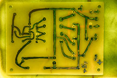
 Photolithography is a complex process used to make integrated circuits and to construct micro-electro-mechanical systems (MEMS) such as accelerometers, pressure sensors and optical switches. It is only employed on flat surfaces that are free of any contaminants. This form of lithography can etch a pattern with a single beam of UV light on a photosensitive chemical. Different geometric shapes can be formed as the film or substrate dissolve. This technique is cost effective, precise, popular and enables small incisions. Other forms of lithography being investigated as an alternative to conventional UV include electron beam, x-ray, extreme ultraviolet and ion projection. It is important to note that the exact shape and size of the film/substrate are controlled by photolithography.
Master Bond has been a leading supplier of adhesives, sealants, coatings to the photolithograph industry. Select grades have been customized to adapt to specific customer needs. As the equipment evolves and becomes more complex Master Bond has helped many key manufacturers stay competitive by navigating new innovative solutions to advance productivity. Adaptation of these adjustments has helped reduce operational expenses and maintenance costs through increased reliability. Additionally Master Bond is devoting much effort in collaborating with key photolithograph companies in developing next generation equipment offering advanced capabilities.
UV curable epoxies such as Master Bond UV15LV1 have been spin coated on silicon wafers, to form claddings. Inverted ridges have then been photolithographically defined on these claddings.
Sources:
1Satsuki Takahashi, Bipin Bhola, Andrew Yick, William H. Steier, Jingdong Luo, Alex K.-Y. Jen, Dan Jin, and Raluca Dinu. Photo-Stability Measurement of Electro-Optic Polymer Waveguides With High Intensity at 1550-nm Wavelength. Journal Of Lightwave Technology, Vol. 27, No. 8, April 15, 2009. Accessed June 2016.
[1]
